Cubic BN has the second highest atomic density (1.68 × 1023 cm-3) and the second highest hardness (70 GPa) and the second highest thermal conductivity (13 W/cmK) just next to diamond. Because of the strong covalent bonds and induced ionicity, cBN even surpasses the most extreme material, diamond, in chemical and thermal stability. Cubic BN resists oxidation at ambient environment up to 1200 oC which is the value as twice higher as the oxidation temperature of diamond. The transformation temperature of sp3 to sp2 BN phase is 1550 oC whereas diamond transform to graphite at 1400 oC.
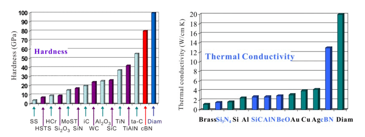
The hardness and thermal conductivity of different materials
Unlike diamond, cBN is chemically inert when it contacts with molten ferrous materials. These extreme properties make cBN the best materials for machining ferrous materials such as tool steels. In addition, cBN has the widest band gap (6.2 ± 0.2 eV) of all III-V compound materials and can be doped for both p- and n-type conductivity. The electronic properties and the thermal stability hint the possibility of utilizing cBN in high speed, high power and high frequency electronic devices.
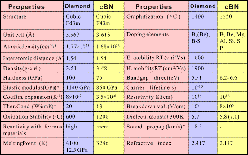
Physical properties of diamond and cBN
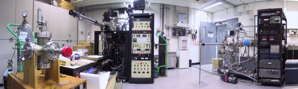
The extreme properties of cBN have prompted material scientists to develop their novel structures and new industrial products. The study on the synthesis and characterization of cBN and diamond started almost together in the early 1960s. To date, cBN has been commercially synthesized in large quantities as powders with sizes ranging from submicron to millimeters by a high-pressure high-temperature (HPHT) method. Abrasive cBN powders are usually cemented by metal binders and formed to fabricate tools of various shapes. Together with HPHT diamond, HPHT cBN has a billion dollars market especially in cutting tools and wear parts. The severe nature of the HPHT methods and the limited size of cBN grains produced, however, prohibit many attractive potential applications of cBN. This is a major motivation for thin film synthesis of both cBN and diamond.
The similarities in structure, properties, technological evolution and application of diamond and cBN suggest that it is worthy to discuss several points related to the synthetic methods of these materials. Diamond films can be prepared in nanocrystalline and polycrystalline forms by using chemical vapor deposition (CVD) methods. CVD diamond films have been already employed in several industrial areas. For example, diamond heat sinks are used in electronic devices. The diamond-coated cutting tools are also commercially available, and they are found to be highly reliable, high-performance and cost-effective tools particularly in machining and cutting hard aluminum alloys. Homoepitaxial diamond single crystals synthesized by CVD are commercially available as well.
However, although synthesis of cBN by low-pressure methods started historically the same time as diamond synthesis, the cBN film quality lags far behind that of diamond, and cBN films have not been implemented into practice so far. A part of the problems is associated with the deposition techniques themselves. Unlike CVD diamond growth, cBN deposition methods require ion assistance (bombardments) which introduces defects in the films and therefore the structure of cBN films are nanocrystalline, highly defective, and contain other BN phases.
(Left) CVD diamond coating for cutting purpose; (Right) Thick CVD diamond film (0.2 mm)
Layered structures
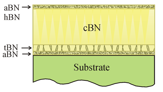
Typical structure of cBN thin films
To overcome the illustrated problems, several approaches have been undertaken including:
Center Of Super Diamond and Advanced Films (COSDAF) is a leading local institution with an international status in the R&D of hard coating especially diamond and cBN. COSDAF has established several methods to deposit thick and adherent cBN thin films with the finianical support from several RGC and ITF projects. COSDAF has acquired comprehensive infrastructures and facilities (deposition systems and material characterization equipments) for development of super-hard coating. CityU is the first and only institution in the world that can prepared, highly pure, thick and uniform cBN film in large area (4 × 4 cm2). And the deposited cBN films show high stability for more than 2 years. The adherent and stable characteristics of the cBN leads to the project of cBN coated tools for practical machining.
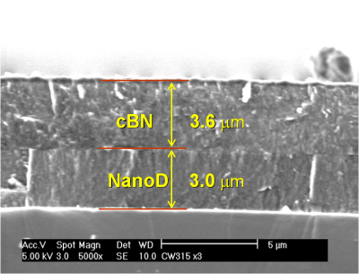
The cross-sectional SEM image of the thick cBN-nanodiamond-Si structure
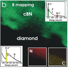
(Right) B (main image), N (inset, lower part, middle), and C (inset, lower part, right) elemental mapping indicating an interface between cubic BN and diamond.
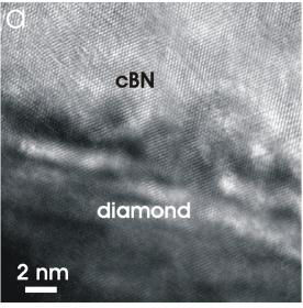
(Left) Cross-sectional HRTEM image of the diamond/cBN interface. The cBN grows directly on diamond with no aBN or tBN layer.
(Left) The diamond coated WC substrate;
(Right) The cBN-diamond deposited on WC inserts.
Preparation of multilayers stems from superlattice structures where two thin layer materials with different properties are stacked periodically to yield the overall properties surpassing that of individual material components. The smallest mismatch in lattice constants (1.3%) and surface energies of diamond and cBN ease the combination of diamond and cBN into multilayer structures. We synthesized nanocrystalline cBN (N-cBN)/nanodiamond (ND) multilayer structure with equivalent layer thickness of ~100 nm on the basal ND film coated silicon substrates. The cBN/ND multilayer film also enhances the mechanical properties of individual layer materials (Hardness of cBN and nanodiamond are 70 and 60 GPa respectively) and the surface of cBN preserves the chemical stability, suggesting the utilization in mechanical protective coatings and tribology.
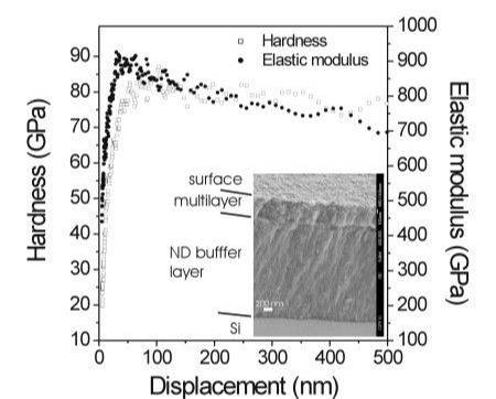
(Right) Dependence of hardness and elastic modulus on displacement measured on a nine-layered N-cBN/ND multilayer
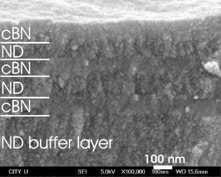
(Left) Cross-sectional SEM micrograph showing the N-cBN/ND multilayer grown on a thick ND buffer layer
The representative articles were selected as the cover of the international journals.
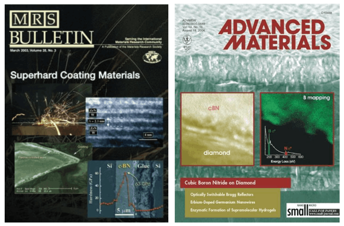
(Left) MRS Bulletin 2003; (Right) Advanced Materials 2004

Drag & Drop Website Builder