Artificial visual system of record-low energy consumption for the next generation of AI
A joint research led by City University of Hong Kong (CityU) has built an ultralow-power consumption artificial visual system to mimic the human brain, which successfully performed data-intensive cognitive tasks. Their experiment results could provide a promising device system for the next generation of artificial intelligence (AI) applications.
The research team is led by Professor Johnny Chung-yin Ho, Associate Head and Professor of the Department of Materials Science and Engineering (MSE) at CityU. Their findings have been published in the scientific journal Science Advances, titled “Artificial visual system enabled by quasi-two-dimensional electron gases in oxide superlattice nanowires”.
As the advances in semiconductor technologies used in digital computing are showing signs of stagnation, the neuromorphic (brain-like) computing systems have been regarded as one of the alternatives in future. Scientists have been trying to develop the next generation of advanced AI computers which can be as lightweight, energy-efficient and adaptable as the human brain.
“Unfortunately, effectively emulating the brain’s neuroplasticity – the ability to change its neural network connections or re-wire itself – in existing artificial synapses through an ultralow-power manner is still challenging,” said Professor Ho.
Enhancing energy efficiency of artificial synapses
Artificial synapse is an artificial version of synapse - the gap across which the two neurons pass through electrical signals to communicate with each other in the brain. It is a device that mimics the brain's efficient neural signal transmission and memory formation process.
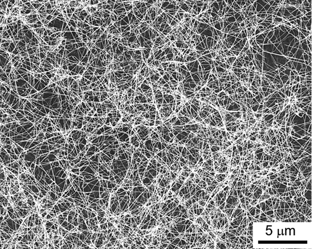
To enhance the energy efficiency of the artificial synapses, Professor Ho’s research team has introduced quasi-two-dimensional electron gases (quasi-2DEGs) into artificial neuromorphic systems for the first time. By utilising oxide superlattice nanowires - a kind of semiconductor with intriguing electrical properties – developed by them, they have designed the quasi-2DEG photonic synaptic devices which have achieved a record-low energy consumption down to sub-femtojoule (0.7fJ) per synaptic event. It means a decrease of 93% energy consumption when compared with synapses in the human brain.
“Our experiments have demonstrated that the artificial visual system based on our photonic synapses could simultaneously perform light detection, brain-like processing and memory functions in an ultralow-power manner. We believe our findings can provide a promising strategy to build artificial neuromorphic systems for applications in bionic devices, electronic eyes, and multifunctional robotics in future,” said Professor Ho.
Resembling conductance change in synapses
He explained that a two-dimensional electron gas occurs when electrons are confined to a two-dimensional interface between two different materials. Since there are no electron-electron interactions and electron-ion interactions, the electrons move freely in the interface.
Upon exposure to light pulse, a series of reactions between the oxygen molecules from environment absorbed onto the nanowire surface and the free electrons from the two-dimensional electron gases inside the oxide superlattice nanowires were induced. Hence the conductance of the photonic synapses would change. Given the outstanding charge carrier mobility and sensitivity to light stimuli of superlattice nanowires, the change of conductance in the photonic synapses resembles that in biological synapse. Hence the quasi-2DEG photonic synapses can mimic how the neurons in the human brain transmit and memorise signals.
A combo of photo-detection and memory functions
“The special properties of the superlattice nanowire materials enable our synapses to have both the photo-detecting and memory functions simultaneously. In a simple word, the nanowire superlattice cores can detect the light stimulus in a high-sensitivity way, and the nanowire shells promote the memory functions. So there is no need to construct additional memory modules for charge storage in an image sensing chip. As a result, our device can save energy,” explained Professor Ho.
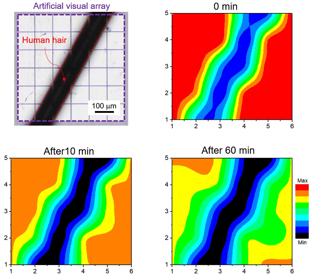
With this quasi-2DEG photonic synapse, they have built an artificial visual system which could accurately and efficiently detect a patterned light stimulus and “memorise” the shape of the stimuli for an hour. “It is just like our brain will remember what we saw for some time,” described Professor Ho.
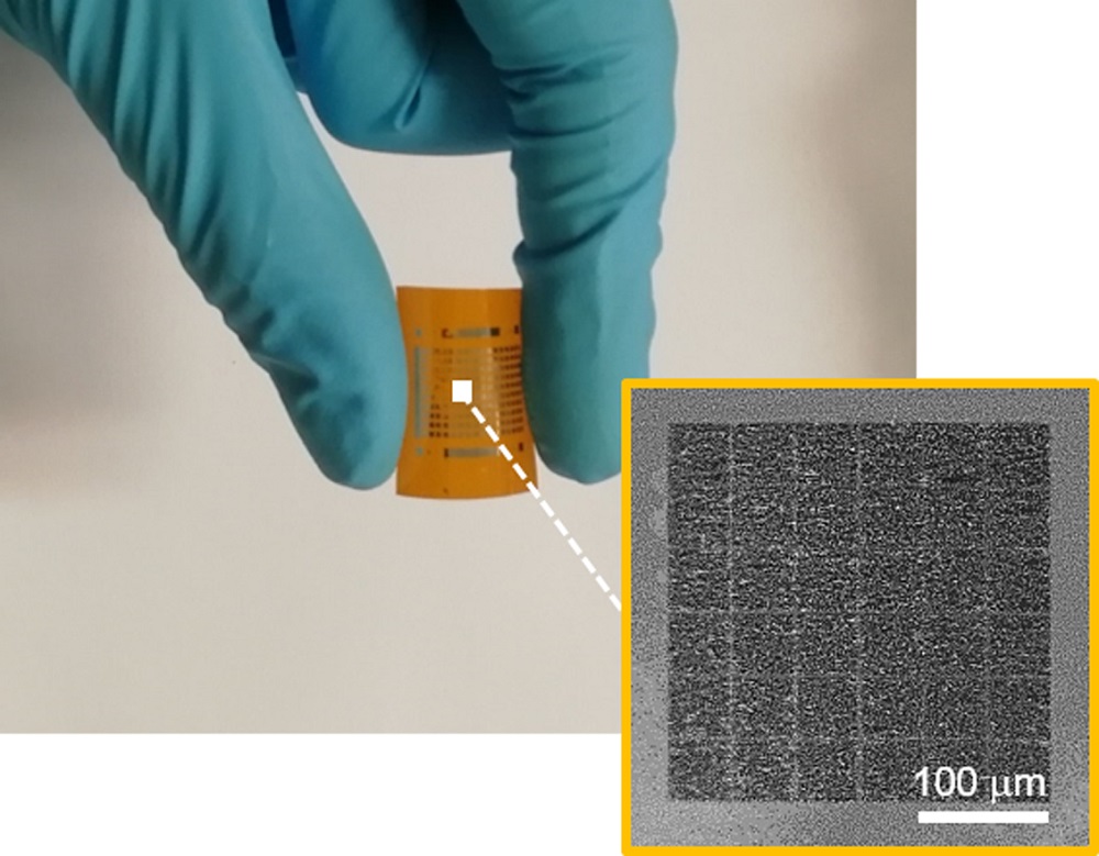
Professor Ho added that the way the team synthesised the photonic synapses and the artificial visual system did not require complex equipment. And the devices could be made on flexible plastics in a scalable and low-cost manner.
Professor Ho is the corresponding author of the paper. The co-first authors are Meng You and Li Fangzhou, PhD students from MSE at CityU. Other team members include Dr Bu Xiuming, Dr Yip Sen-po, Kang Xiaolin, Wei Renjie, Li Dapan and Wang Fei, who are all from CityU. Other collaborating researchers come from University of Electronic Science and Technology of China, Kyushu University, and University of Tokyo.
The study received funding support from CityU, the Research Grants Council of Hong Kong SAR, the National Natural Science Foundation of China and the Science, Technology and Innovation Commission of Shenzhen Municipality.
DOI number: 10.1126/sciadv.abc6389