Mixed-Dimensional Transistors Enable High-Performance Multifunctional Electronic Devices
Downscaling of electronic devices, such as transistors, has reached a plateau, posing challenges for semiconductor fabrication. However, a research team led by materials scientists from City University of Hong Kong (CityU) recently discovered a new strategy for developing highly versatile electronics with outstanding performance, using transistors made of mixed-dimensional nanowires and nanoflakes. This innovation paves the way for simplified chip circuit design, offering versatility and low power dissipation in future electronics.
In recent decades, as the continuous scaling of transistors and integrated circuits has started to reach physical and economic limits, fabricating semiconductor devices in a controllable and cost-effective manner has become challenging. Further scaling of transistor size increases current leakage and thus power dissipation. Complex wiring networks also have an adverse impact on power consumption.
Multivalued logic (MVL) has emerged as a promising technology for overcoming increasing power consumption. It transcends the limitations of conventional binary logic systems by greatly reducing the number of transistor components and their interconnections, enabling higher information density and lower power dissipation. Significant efforts have been devoted to constructing various multivalued logic devices, including anti-ambipolar transistors (AAT).
Anti-ambipolar devices are a class of transistors in which positive (holes) and negative (electron) charge carriers can both transport concurrently within the semi-conducting channel. However, existing AAT-based devices utilize predominately 2D or organic materials, which are unstable for large-scale semiconductor device integration. Also, their frequency characteristics and energy efficiency have rarely been explored.
To address these limitations, a research team led by Professor Johnny Ho, Associate Vice-President (Enterprise) and Associate Head in the Department of Materials Science and Engineering at CityU, embarked on research to develop anti-ambipolar device-based circuits with higher information density and fewer interconnections, and explore their frequency characteristics.
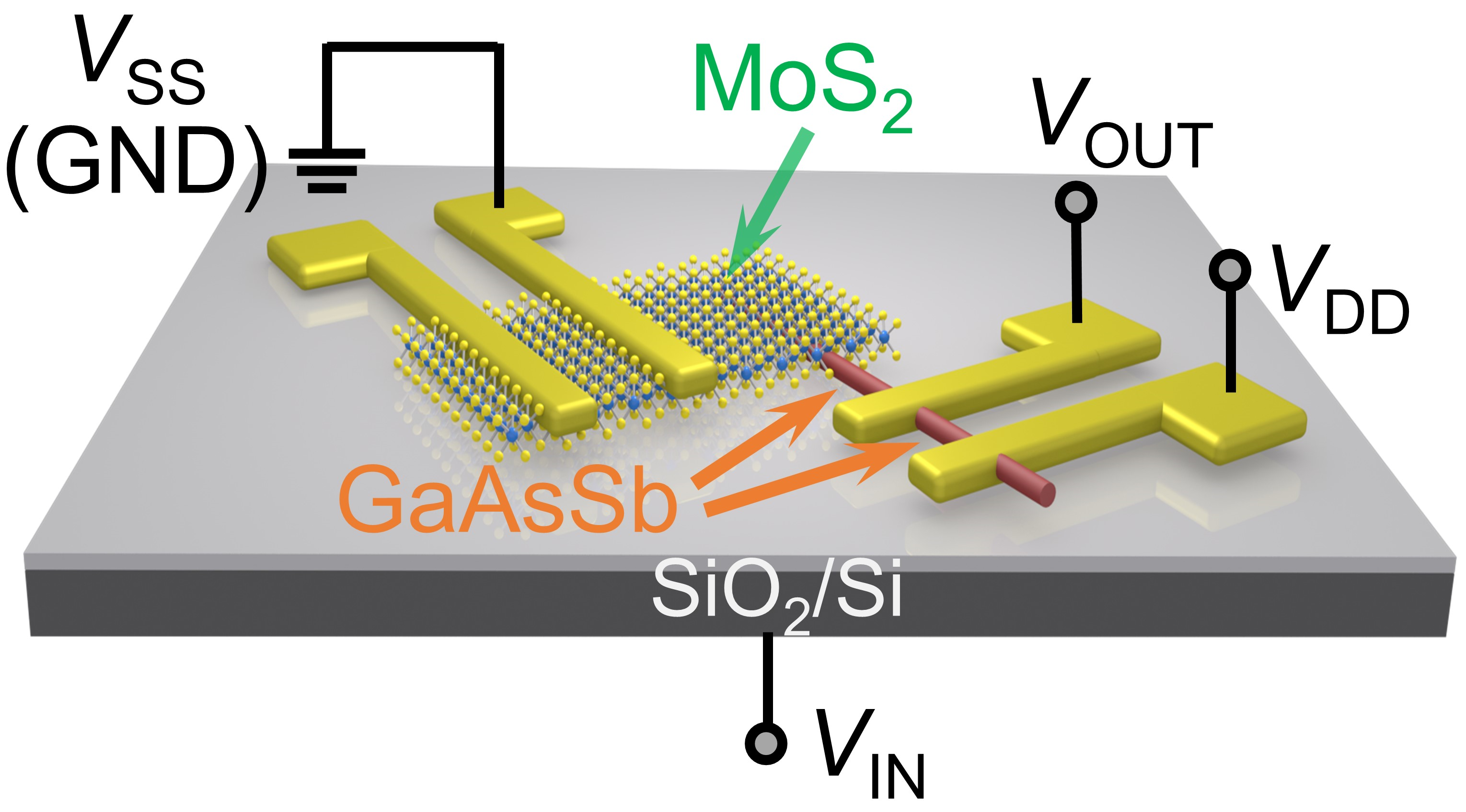
The team created an advanced chemical vapour-deposition technique to create a novel, mixed-dimensional hetero-transistor, which combines the unique properties of high-quality GaAsSb nanowires and MoS2 nanoflakes.
The new anti-ambipolar transistors had exceptional performance. Owing to the strong interfacial coupling and band-structure alignment properties of the mixed-dimensional GaAsSb/MoS2 junction, the hetero-transistor has prominent anti-ambipolar transfer characteristics with the flipping of transconductance.
The flipping of transconductance doubles the frequency in response to the input analog circuit signal, greatly reducing the number of devices required compared to conventional frequency multiplier in CMOS technology.
“Our mixed-dimensional, anti-ambipolar transistors can implement multi-valued logic circuits and frequency multipliers simultaneously, making this the first of its kind in the field of anti-ambipolar transistor applications,” said Professor Ho.
The multi-valued logic characteristics simplify the complicated wiring networks and reduce chip power dissipation. The shrinking of device dimensionality, together with the downscaled junction region, render the device fast and energy efficient, resulting in high-performance digital and analog circuits.
“Our findings show that mixed-dimensional anti-ambipolar devices enable chip circuit design with high information storage density and information processing capacity,” said Professor Ho. “So far, most researchers in the semiconductor industry have focused on device miniaturization to keep Moore's law rolling. But the advent of the anti-ambipolar device shows the comparative superiority of the existing binary logic-based technology. The technology developed in this research represents a big step towards next-generation multifunctional integrated circuits and telecommunications technologies.”
The research also opens the possibility of further simplifying complex integrated circuit designs to improve performance.
The mixed-dimensional anti-ambipolar device’s transconductance-flipping feature has shown the possibility of versatile applications in digital and analog signal processing, including ternary logic inverters, advanced optoelectronics and frequency-doubling circuits. “The new device structure heralds the potential of a technological revolution in future versatile electronics,” added Professor Ho.
The findings, titled “Multifunctional anti-ambipolar electronics enabled by mixed-dimensional 1D GaAsSb/2D MoS2 heterotransistors”, were published in the scientific journal Device.

Dr Wang Wei, a PhD graduate in the MSE at CityU, is the first author, and Professor Ho is the corresponding author. Collaborators include Dr Yip Sen-po, a CityU PhD graduate, supervised by Professor Ho, who is currently working in Kyushu University in Japan.
The research was funded by the Research Grants Council of the Hong Kong Special Administrative Region and the Shenzhen Municipality Science and Technology Innovation Commission.