Breakthrough in Low-Temperature Copper Bonding Technology Enables Next-Generation Electronics Manufacturing
Researchers from the City University of Hong Kong (CityUHK) have achieved a significant breakthrough in electronic packaging technology by developing an innovative nanocrystalline (NC) copper material that enables direct copper-to-copper bonding at lower temperatures. This advancement opens new possibilities for advanced chip design, which is crucial for many next-generation technologies.
The research team led by Professor Shien-Ping Feng from the Department of Systems Engineering has successfully developed a nanocrystalline (NC) copper material for direct copper-to-copper (Cu-Cu) bonding that works at lower temperatures. This breakthrough combines excellent bonding quality with reduced temperature requirements, making it an attractive solution for advanced electronic packaging. The technology is particularly valuable for industrial mass production, as it requires both less heat and less time to create reliable bonds.
The findings were recently published in Nature Communications, titled “Nanocrystalline copper for direct copper-to-copper bonding with improved cross-interface formation at low thermal budget”.
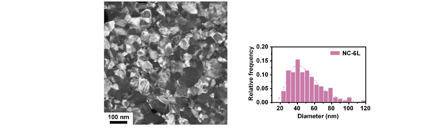
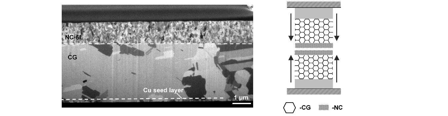

Using NC copper for direct Cu-Cu bonding is a promising technology for advanced electronic packaging. However, it faces two key challenges. First, it contains many grain boundaries where impurities tend to concentrate, making it difficult for grains to grow sufficiently when heated at lower temperatures. Second, when the material is heated gently, the NC grains grow on the top surface but can not grow at the bottom, leading to the formation of voids near the bottom copper seed layer. These issues make it harder to create strong and reliable bonds.
The team overcomes the challenges by developing a strategic dual-layer design where the coarse-grain layer acts as an impurity sink, facilitating controlled impurity diffusion and preventing void formation near the copper seed layer.
“By developing additives, we can electroplate NC copper with uniform nanograin sizes and low impurities, enabling rapid grain growth at low temperatures. We found that a single NC layer is ineffective for Cu-Cu bonding, so propose a dual-layer structure with NC Cu over a coarse-grain (CG) layer,” Professor Feng explains.
The ability to bond copper at lower temperatures opens new possibilities for advanced chip design. It allows engineers to integrate different types of chips - especially those sensitive to heat - into compact, high-density 3D structures. This breakthrough enables the development of more sophisticated chip architectures, which are crucial for advancing technologies like artificial intelligence, high-performance computing, 5G networks, and augmented/virtual reality systems. Moving forward, the team will work with semiconductor manufacturers to integrate this new bonding technique into current production processes, including established methods like thermocompression and hybrid bonding.
For inquiries, please contact Professor Shien Ping Feng, the Department of Systems Engineering and Department of Mechanical Engineering at CityUHK, by email at shiefeng@cityu.edu.hk.