Physics and Materials Science PhD student
Mr Mei Yongfeng has won the 2004 Young Scientist Award from the
European Materials Research Society (E-MRS) in recognition of his outstanding research in microelectronics technology. At the E-MRS 2004 Spring Meeting, held 24-28 May, in
Strasbourg, France, Mr Mei received his certificate.
"Microelectronics technology is an exciting interdisciplinary research area for studying materials, and the molecular components of electronics," Mr Mei said. It is fascinating to me and holds great promise for the future advancement of processors in microelectronics industry.”
The largest conference in Europe for presentation of new scientific ideas and results in materials R&D, the E-MRS 2004 Spring Meeting included 21 technical symposia, each of which named one or two 'Young Scientist' winners. Mei submitted his paper to the symposium called “Current Trends in Nanoscience from Materials to Applications”. His work first won him the Graduate Student Award and then clinched one of the two Young Scientist Awards of that symposium. E-MRS panel adjudicators commended his work as thorough and having great value to future nanoscience study.
A novel fabrication method
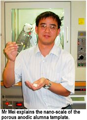
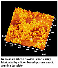
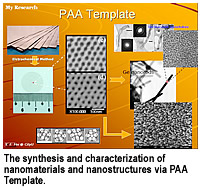
In conducting his research, Mei employs a self-organized effect to fabricate a porous anodic alumna (PAA) template, which shows a nanopore array with different size and ordered arrangement. He uses the template-assistant fabricated method to synthesize semiconductor nanomaterials and their arrays, as well as other functional nanostructures, which cannot be produced in nano-scale by conventional microelectronics technology.
Mei's research provides microelectronics technology with scientific explanations and possible alternatives for its future development, especially related to the components, energy band gap and defects of semiconductors. By using semiconductor nano materials to assemble
high-performance nano devices, he attempts to provide possible alternatives to replace conventional transistors. This R&D area has been pursued by leading chip-making corporations such as
Intel and
IBM. Successful application of the research would enhance the development of high technology products such as the central processing units in computers.
Revelling in the world of nanoscience
Mr Mei treasures the E-MRS Meeting as an eye-opening experience for exchanging ideas with top researchers and industry practitioners. "Through participating in the symposium, I have gained insight and explored collaboration opportunities with research students from other univeristies," he said. "It has also boosted my confidence for further study in the field."
Mei has been enamored of nanotechnology since he was a research student at
Nanjing University. There, he specialized in silicon-based light-emitting nanomaterials. Mei decided to continue his pursuit of nanotechnology at CityU once he completed his Master’s degree in 2002. At that time, his teacher,
Professor Wu Xinglong, came to CityU as Visiting Fellow and recommended that Mei study a PhD degree here. With offers from other leading universities in
Hong Kong, he finally decided to study at CityU. “At CityU, we have excellent faculty members and state-of-the-art laboratories.” He said he has also benefited from the strong research ethos of the
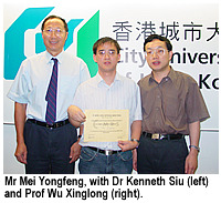
Department of Physics and Materials Science (AP). His PhD supervisor
Dr Kenneth Siu, AP Associate Professor, has encouraged him to develop new ideas and given him good advice for his research.
“Mei’s success is due to his diligence and innovative ideas,” Dr Siu remarked. Dr Siu said that at CityU Mei's ideas became more mature. “Mei's receiving the award attests to the fact that CityU provides the best environment and technologies to nurture young talents in the field,” Dr Siu said. “Nanotechnology is so fascinating a research area that every tiny aspect of it can have tremendous impact," Mei added. "I explore the world of nanoscience just like an astronomer exploring the beauty of the galaxy.” He likened the nano component of objects to wonderful landscapes, cityscapes, mountains and seas of the world. “In application, the technology has great potential to improve daily life. I enjoy looking into the tiny components and working out alternative solutions to the current findings.”
The European Materials Research Society was founded in 1983 in Strasbourg. It aims to foster international cooperation and exchange on the latest developments in materials research. The E-MRS Young Scientist Award aims to encourage materials science research students. The total attendance at this year's Spring Meeting was over 2,000, including practitioners from the materials science industry, academics, scientists, and postgraduate students from prestigious universities such as the Max-Planck Research Institute in Germany, the UK’s University of Cambridge, Oxford University, and Stanford University in the US.